The Hidden Lifespan Killer: How Solder Temperature Dictates Your PCBA's Fate
Ever wonder why some electronics seem to chug a

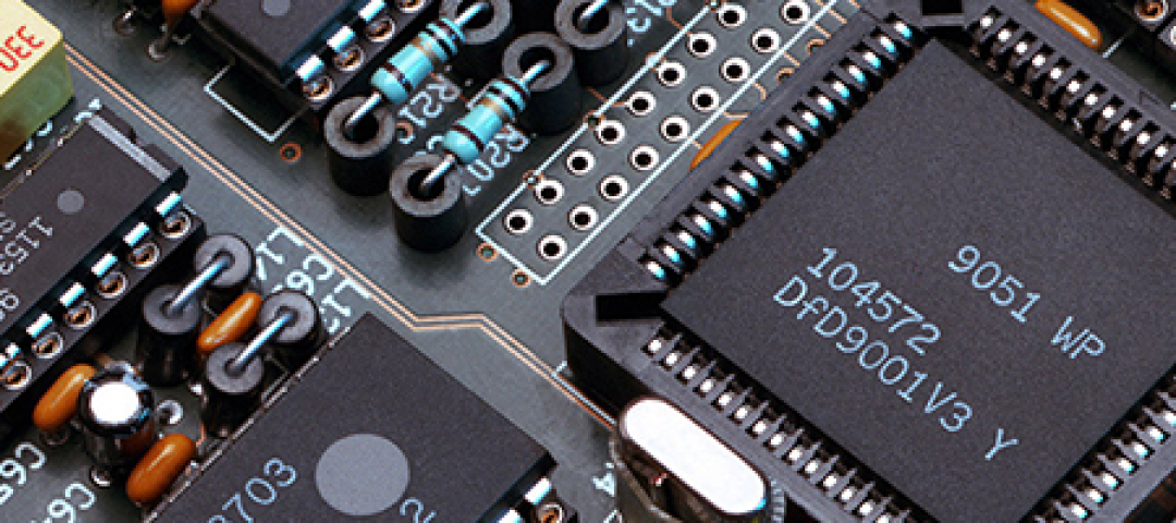
Printed circuit board(PCB) is a very significant part of electronic equipment. With the popularity of electronic products, it is meaningful to understand every step of the circuit card assembly process. In this article today, we will introduce you to the specific steps to complete PCB assembly(PCBA).
1.PCB Design
Creating a design is the first step of printed circuit board services, we often use computer aided design (CAD) software to design the schematic and layout, during the design process, the designer needs to comply with the design rules, ensure the correct component placement and connection, define the width of the trace, layer stack-up and component space.
2.Generating and Reviewing Gerber Files
Once the design is complete, the next step is to export a Gerber file that contains critical details about the PCB layer and copper pattern. This step guarantees that subsequent production can be completed more precisely according to the design. You can also send your Gerber file to XW and we will review and verify it for you.
3.PCB Manufacturing
The third step in production is to turn the design into a solid PCB.
You will gain a completed standard PCB after below six procedures,including: 1. Select the substrate and copper clad laminates; 2. Apply photoresist and photomask; 3. Etch to create traces; 4. Through hole assembly and through hole drilling; 5. Electroplating and chemical deposition; 6. Apply solder mask and silk screen.
4.Material source
Material Procurement is the fourth step of production. At this stage, we will first make the required bill of materials (BOM) according to your needs, which will greatly improve our purchasing efficiency and reduce costs. We will then purchase the high quality electronic components needed to complete the PCB project from a stable and reliable supplier according to the list.
5.preparing Component
For PCB manufacturing assembly preparation and organization of electronic components, there are two widely used methods: surface mount technology (SMT) and through hole technology (THT).
Different from THT technology, SMT technology requires the use of solder paste, so there are several processes:
(1.) PCB Loading:Loading machine will be used in the SMT, and its main role is to align the PCB with the solder paste printer
(2.) Stencil Production:Next we need to create a template, this step is so that the solder paste can be precisely applied to the surface mount components of PCB.
(3.) Solder Paste Application: In this step, we need to pay attention to the amount of solder paste, because improper use will lead to defects. First we need to push the PCB into alignment with the template, and then use the squeegee to spread the appropriate amount of solder paste onto the pad.
6.Component Placement
In this step, we will use a high precision pick-and-place machine to place the part in the specified position according to the CAD layout.
7.Soldering
After the location of the component is placed, we will welding, the general common welding methods are mainly the following three, and specific use of which need to be determined according to the specific assembly technology:
(1.) Reflow Soldering:
Usually suitable for SMT, In order to connect the components to the board, the PCB will be placed in a reflow furnace to liquefy the solder paste.
(2.) Wave Soldering:
Usually suitable for THT. By molten solder wave, the PCB attaches to exposed pads and component leads.
(3.) Manual Soldering:
Usually suitable for THT, the parts are manually welded by a skilled technician with a soldering iron
8.Post-Solder Inspection
This step of testing is designed to check the solder quality of the PCB, in this step, automatic optical inspection (AOI), X-ray inspection will be used, or manual inspection by experienced technicians.
9.Testing and Debugging
The purpose of this step is to test the functionality of the assembly smt, and the techniques commonly used include online testing, flying needle testing, and functional testing.
10.Final Assembly and Packaging
Final pcb board assembly manufacturing and Packaging is the last step in the production process where all the necessary connectors, radiators, housings and other hardware were connected and tightly packed for shipping.
Conclusion
For you, understanding the intricacies of this process will help you create high-quality electronic devices that pave the way for the success of your projects and innovations.
For us, manufacturing products by strictly following the final steps of printed circuit board assembly manufacturer ensures efficient production and full product functionality.
XW With more than decade of experience in the Printed circuit assembly industry, we can customize the most suitable, advanced SMT PCB board and PCBA service for you. For any inquiries or requirements of custom pcb fabrication and assembly needs, please don’t hesitate to contact us for more information We will respond within 2 hours and offer you the most effective circuit board assembly solutions.