The Hidden Lifespan Killer: How Solder Temperature Dictates Your PCBA's Fate
Ever wonder why some electronics seem to chug a
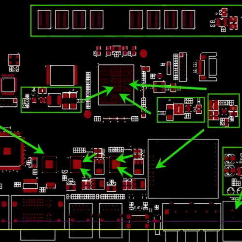
PCB Design and Layout
PCB design and layout is the process of creating the physical layout of a printed circuit board to connect electronic components in a circuit.
PCB design and layout is the process of creating the physical layout of a printed circuit board to connect electronic components in a circuit. This process involves designing the placement of electronic components, routing the electrical connections between them, and defining the shape and size of the circuit board. XW Technology offers comprehensive printed circuit board design services, with an experienced design team specializing in a wide range of PCB designs, from simple to complex.
12+ years experience and 300+ engineers working with overseas projects
ISO9001:2015, ISO14001, ISO13485, ROHS, and UL
designing, engineering, prototyping, and production and after-sales services
Coverage of over 150 countries and over 3,600 customers
Respond to your request within one hour, we provide 7/24 hours support for customers in different time zones
SMT lines + Automatic plug-in production line + Wave soldering lines + Assembly lines

Ever wonder why some electronics seem to chug a

In electronics manufacturing, the
We provide customized PCB assembly solutions, from PCB design, prototyping, and manufacturing, to assembly and testing, our one-stop service


