Application of MES Systems in PCBA Factories
With the advancement of Industry 4.0 and the rapid development of intelligent
PCBA (Printed Circuit Board Assembly) inspection is a crucial process to ensure the quality of assembled printed circuit boards. The inspection process generally includes the following steps:
Incoming Material Inspection
Objective: Ensure that the raw materials and components used in PCBA production meet quality standards to avoid product quality issues caused by incoming material problems.
Content:
1.PCB Bare Board Inspection: Check the appearance of the PCB, including scratches, notches, shorts, open circuits, etc.; measure PCB dimensions and thickness to ensure they meet design requirements; inspect the electrical performance of the PCB, such as circuit continuity and insulation performance.
2.Electronic Component Inspection: Conduct visual inspections of electronic components like resistors, capacitors, inductors, chips, etc., to check for damage, deformation, or pin oxidation; use professional instruments to measure component parameters such as resistance, capacitance, and inductance to ensure they are within specification limits; verify the model and specifications of the components against the BOM (Bill of Materials).
Solder Paste Printing Inspection
Objective: Ensure the quality of solder paste printing, including the quantity, position, and shape of the solder paste, to lay a good foundation for subsequent soldering processes.
Content:
a. Solder Paste Quantity Inspection: Measure the thickness and volume of solder paste on PCB pads using a solder paste thickness tester or optical inspection equipment to ensure that the amount of solder paste is uniform and meets process requirements.
b. Solder Paste Printing Position Inspection: Check whether the solder paste is accurately printed on the pads and if there is any misalignment or offset. This can be done through optical inspection or manual visual inspection.
c. Solder Paste Shape Inspection: Observe whether the solder paste shape is regular and whether there are any issues like collapsed edges or bridging, which can lead to soldering defects like short circuits.
Placement Inspection
Objective: Ensure that electronic components are accurately placed on the PCB with correct positioning and orientation.
Content:
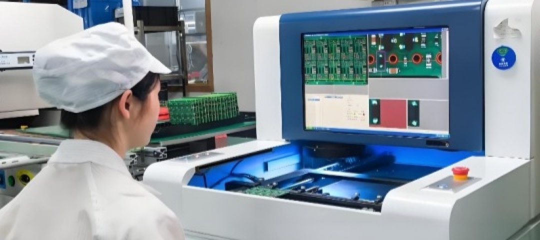
1.Component Placement Position Inspection: Use optical inspection equipment, such as an AOI (Automated Optical Inspection) system, to check whether components are placed in the correct pad positions and if the deviation is within acceptable limits.
2.Component Placement Orientation Inspection: Confirm whether the polarity and orientation of components such as capacitors, diodes, and integrated circuits are correct, as incorrect orientation can cause the circuit to malfunction.
3.Placement Height Inspection: Check if the height of the placed components on the PCB is consistent. Incorrect placement height may affect soldering quality or cause problems in later assembly steps.
Reflow Soldering Inspection
Objective: Monitor the temperature profile during reflow soldering to ensure soldering quality and avoid defects such as cold joints, shorts, or solder balls.
Content:
a. Temperature Profile Inspection: Use a temperature tester and place thermocouples on the PCB to measure temperature changes during reflow soldering at different stages. Analyze whether the temperature profile meets soldering process requirements, including parameters such as preheat temperature, soak time, peak temperature, and cooling rate.
b. Soldering Appearance Inspection: After reflow soldering, inspect the quality of the solder joints through manual visual inspection or AOI equipment. Check if the solder joints are full and shiny and if there are any defects like cold joints, missed soldering, short circuits, or solder balls.
c.Solder Joint Strength Inspection: For some key solder joints, perform mechanical strength tests such as pull tests or shear tests to ensure the solder joints are firm and reliable.
Through-hole Components and Wave Soldering Inspection
Objective: For PCBA with through-hole components, this step ensures the quality of through-hole soldering and wave soldering.
Content:
1.Component Placement and Orientation Inspection: Check whether through-hole components are inserted into the correct holes, whether the orientation is correct, and whether the leads are bent or deformed.
2.Wave Soldering Quality Inspection: Inspect the appearance of the solder joints for defects such as missed soldering, cold joints, bridging, or solder spikes. Check the soldering connection between the component leads and PCB pads for firmness, which can be done through visual inspection or AOI equipment.
Functional Testing
Objective: Perform comprehensive functional tests on the PCBA after assembly to verify whether it can operate normally and if its functions meet design requirements.
Content:
Electrical Performance Testing: Use multimeters, oscilloscopes, signal generators, and other testing instruments to measure various electrical parameters of the PCBA, such as voltage, current, resistance, frequency, and waveform. Ensure they meet design specifications.
Functional Module Testing: Test the individual functional modules of the PCBA based on its characteristics, such as communication, data processing, or control functions, ensuring each module works as expected.
Interface Testing: Test the electrical performance and communication functionality of interfaces like USB, serial ports, and Ethernet ports. Ensure they can communicate and interact with external devices correctly.
Appearance Inspection
Objective: Perform a final inspection of the overall appearance of the PCBA to ensure that the product meets quality standards without obvious defects or blemishes.
Content:
Overall Appearance Check: Inspect the PCBA surface for cleanliness, ensuring there are no stains, solder residues, or debris. Check for PCB warping or deformation, as excessive deformation could affect subsequent assembly and usage.
Silkscreen Inspection: Verify that the silkscreen on the PCBA is clear and complete, that characters and labels are correct, and that there are no missing or incorrect prints.
Pre-packaging Inspection
Objective: Perform final spot checks or full checks before packaging and shipment to ensure that the products delivered to customers are of qualified quality.
Content:
Repeat of Some Inspections: Commonly, the appearance and electrical performance tests are repeated to ensure that no damage or new defects occurred during packaging.
Packaging Integrity Check: Ensure that the packaging of the PCBA complies with requirements, such as the use of appropriate packaging materials, proper sealing, and correct labeling.
This detailed inspection process ensures that the PCBA meets both functional and quality standards before it is delivered to customers.
16+ years experience and 300+ engineers working with overseas projects
ISO9001:2015, ISO14001, ISO13485, ROHS, and UL
designing, engineering, prototyping, and production and after-sales services
Covered 150+ countries and 3600+ customers
Reply to your inquiry within 1 hours, we provide 7/24 hours support for customers in different time zones
SMT lines+Automatic plug-in production line+Wave Soldingave Lines+Assembly lines

With the advancement of Industry 4.0 and the rapid development of intelligent

With the continuous development of the electronics manufacturing industry, PC


We provide customized PCB assembly solutions, from PCB design, prototyping, and manufacturing, to assembly and testing, our one-stop service