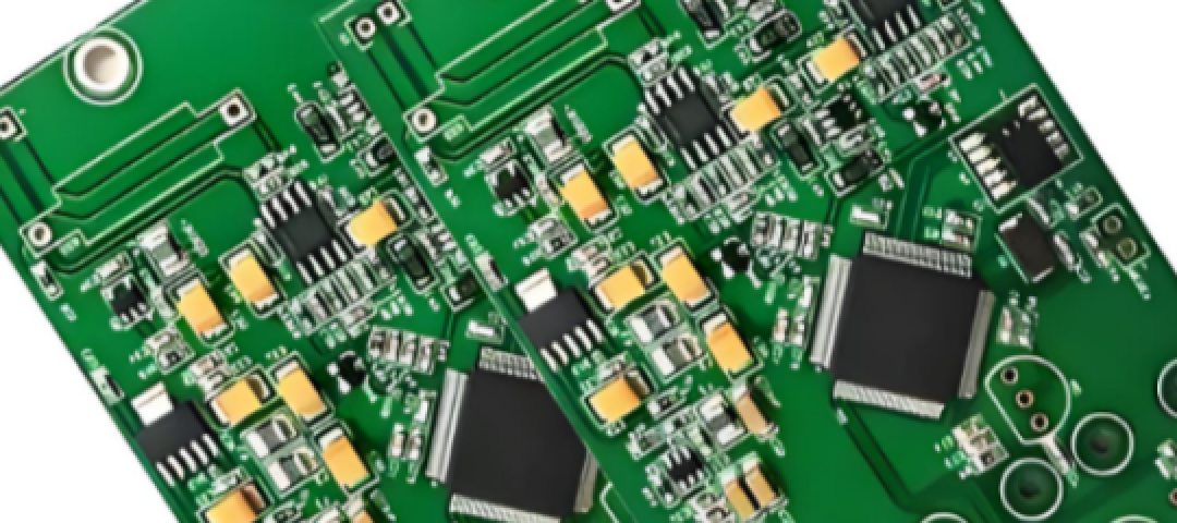
The Hidden Lifespan Killer: How Solder Temperature Dictates Your PCBA's Fate
Ever wonder why some electronics seem to chug a

The modern electronics such as mobile, IPAD, mobile watch enrich our lives, and the PCB, Printed Circuit Board is the core of the electronics, and then PCB assembly(PCBA) in order to make the electronics function normally. PCBs can be made up of up to 40 layers, and the common material is Fr4, and widely applied into nearly all industries.
1.The Importance of PCB Layers
Electrical Connectivity: The layer structure plays a vital role on the electrical performance and function of the PCB, so by distributing conductive wires across multiple layers, the signal flow can be effectively guaranteed, and the interference is greatly reduced, so that the PCB is suitable for more and more complex situation.
Space minimization: Stacking layers vertically helps shrink the whole PCB size and maximize the use of space, which makes the PCB play a greater role in the limited space of miniaturized electronic devices including wearables, smartphones, and Internet of things devices.
2. Different Types of PCB Layers
(1.)Signal Layers: The main conductive layer which is responsible for transmitting electrical signals between components is the signal layer. Comprised of copper wires connecting various components, the signal layer ensuring accuracy and stable signal transmission and routing, and the circuit's complexity and design needs ultimately determine the number of signal layers.
(2.)Ground plane: The component provides stable energy in the PCB is the power supply, and the layer dedicated to the signal return path reference is the ground plane. These two work together to ensure consistent power distribution across the PCB and cut noise and voltage drop. As a low-impedance path dedicated to the return current, the ground plane helping to increase signal accuracy and reduces electromagnetic interference (EMI) throughout the PCB operation.
(3.)Internal Layers: The inner layer is usually located between the outer signal layers of the multi-layer PCB. The inner layer allows PCB design to be more flexible and complex, because it plays many important roles in the entire PCB including power distribution, control impedance wiring, shielding noise from sensitive signals and providing more routing space.
3. Factors to Pay Attention to In PCB Layer Design Process
(1.)Signal Quality: The key to maintaining signal integrity is proper trace routing and layer stacking, so we need to carefully consider the arrangement between layers to ensure signal quality during PCB operation. At the same time, we need to note that controlling impedance routing at a specific layer is necessary for high-speed signals,while sensitive signals can be protected from noise interference with added shielding layers.
(2.)Power Distribution: One of the most important factors in ensuring the operational stability of electronic circuits is proper power distribution. The suitable design of the power supply and ground plane can effectively reduce voltage drop and noise, and stable power supply to the PCB board, which shows that the balance of the position of the power supply and ground plane plays a great role in avoiding coupling effects and improving signal quality.
(3.)Thermal Management: Efficient thermal management is also crucial for PCBS. By combining the hot through hole and the copper plane together, the speed of heat dissipation from the component can be greatly increased, preventing the operation or other quality problems caused by product overheating, ensuring the stability of the PCB, and bringing a good product experience to the user.
(4.)Manufacturer: The cost and complexity of PCB manufacturing will be great influenced by the number of layers and arrangement, so the PCB manufacturer's ability to handle PCB layer stacking and the overall design control is particularly important, because it will have a significant impact on the efficiency of the entire PCB production process. At the same time, feasibility should also be taken into account, so as to ensure the efficient completion of production without reducing efficiency
Conclusion
The PCB layer provides the basis for the interconnection and function of electronic components. With a well designed cascading structure, space can be maximized, electrical connections can be more stable, and the overall performance of electronic devices can be significantly improved.
For any inquiries or requirements of the printed circuit card assembly, manufacturing, please don’t hesitate to contact us for more information. As a reliable PCB board and PCBA manufacturer, Shanghai XW is rich experience in the printed circuit assembly industry, we will customize the most suitable, advanced PCB and PCBA service for you.